


Experiment
Wafer bonding using resist
While processing to thin wafers is needed, various methods exist for bonding and adhesion to the support substrate.
However, none of them require new facilities or can not be easily introduced in terms of cost.
So, we tried challenging to bond using a resist that can be handled easily and can be peeled off with a chemical solution.
What will be the result?
We will use 4 inch wafer this time.
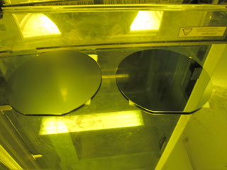
Attempt to bond the mirror surface and etched surface using a resist.
Apply resist with spin coater and bake.
End of baking.
It seems to be bonded for the time being.
The position of the two wafers are misaligned (for complete manual work).
It is a future task.
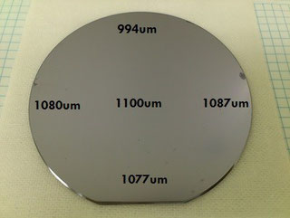
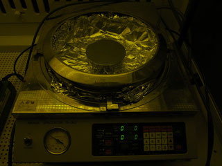
We measured the thickness after bonding. There are variations, parallelism is not good.
This is also a future task.
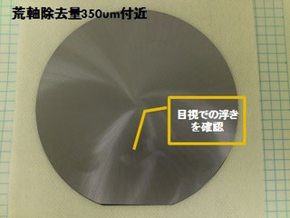
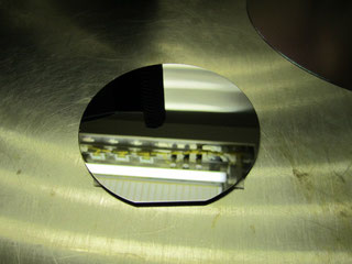
CMP was applied to check the bonding strength.
Floating (peeling) was partially confirmed at the time of removed thickness 350um, but the majority remain bonded.
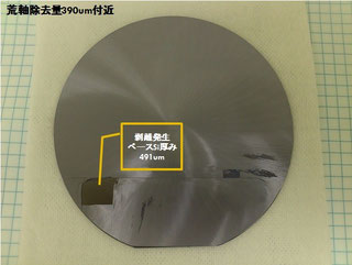
Continuing CMP, Si peeled off partially and cracked at the time of removed thickness around 390um.
Summary
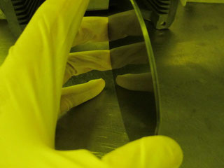
It is necessary to improve the alignment and parallelism at the time of bonding, but is not the strength of the bonding fairly good?
We expected that cracks and peeling occurred at the moment CMP was applied, but it was possible to hold to a certain extent.
We feel the possibility of a process with less stress.
Based on the result of this time, we will proceed with in-house experiments.
Please also see this page for CMP.


