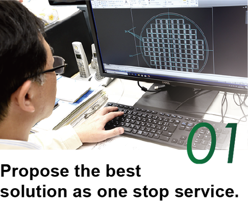
ASSIST-NAVI CORPORATION provides contract processing service specialized to MEMS/Semiconductor R&D as customer's second test lab.

Need help with the following?
Another company told me that small-scale production is not supported.
The optimal material selection and processing method for development cannot be found.
For research and development Insufficient equipment, human resources and time.
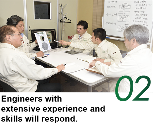
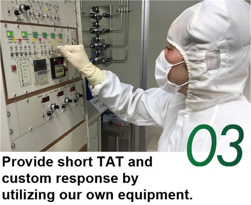
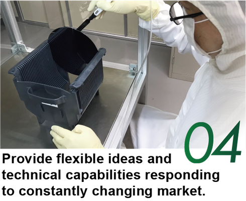
ASSIT-NAVI supports customers with four strengths and technical capabilities

Film formation processing
In our company, sputtering, vacuum deposition, ion From various PVD such as plating, it is represented by TEOS film. We propose the most suitable method from the abundant film forming method to CVD.
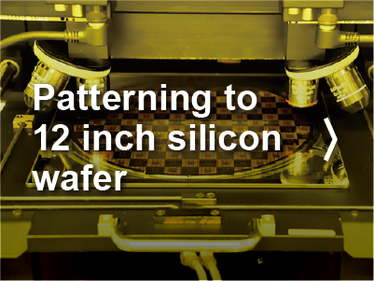
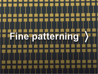
Patterning
Semiconductor element, MEMS structure, plating, etching (Deep-RIE, As a resist patterning method for Dry & Wet) Exposure / development with toner, stepper and EB is possible.
Etching process
This technology is indispensable for semiconductor and MEMS substrate processing. Glass craft It can be used in any field, but two processes, Dry and Wet Has been established, and patterning of various materials is possible.
Semiconductor plating processing
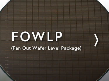
Rewiring and bump plating service to WLP (Wafer Level Package) Screw. Corresponding to each wafer size, Cu pillar, solder bump, low We accept melting point bumps and various bumps.
CMP processing
CMP(Chemical Mechanical Polishing)is
an essential technology for manufacturing multi-layer wiring boards.
We will introduce the scope of application of CMP with processing examples.
TEG wafer
PKG development, packaging method development, packaging & inspection equipment development, material development, etc. Standard TEG Wafer for evaluation is available. customer's We also produce TEG wafers (chips) tailored to your application.
Other
In addition, nanoimprint using lithography and Ni electroforming technology Providing molds for imprinting, polishing, dicing, laser processing are also available

Contact Us
If you have any questions or proporsals
Please feel free to contact us.


Related Links