


Patterning
We can expose and develop with aligners, steppers, EB as resist patterning method for semiconductor elements, MEMS structure, plating, etching (Deep-RIE, dry and wet).
We have various resists for positive type, negative type, dry film, thin film, thick film. Patterning of polyimide is also possible. expose and develop with aligners, steppers, EB as resist patterning method for semiconductor elements, MEMS structure, plating, etching (Deep-RIE, dry and wet).
We have various resists for positive type, negative type, dry film, thin film, thick film. Patterning of polyimide is also possible.
Aligner
- Available for 3 to 12 inch.
- 1 x contact exposure
- Reverse taper pattern for lift-off
- Back side alignment
- In addition to resist, low stress insulating resin can be patterned.


Stepper
- i-line, KrF, immersion available.
- Available for 4 to 12 inch (3 inch or less is consulted separately).
- i-line stepper has high throughput of 1 shot 44mm square.
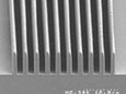
High aspect resist, thick film resist forming
- High aspect ratio resist (for wiring forming).
- Thick film resist (for Cu pillar)
- Other handling high aspect ratio resist for Ni electroforming.

Laser direct drawing
- applicable up to circuit board size 610 mm x 510 mm.
- Alignment (three kinds of red, green, infrared)
- High throughput.
- Mask unnecessary for direct drawing.
- L & S 8um.
EB (direct drawing)
-
Patterning of 80 nm or less is possible.


