About CMP
CMP (Chemical Mechanical Planarization) is an indispensable technology for fabricating multilayer wiring wafers. This page introduces the scope of CMP application, including processing examples.
Purpose of CMP
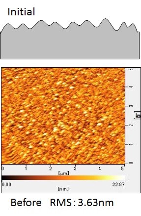
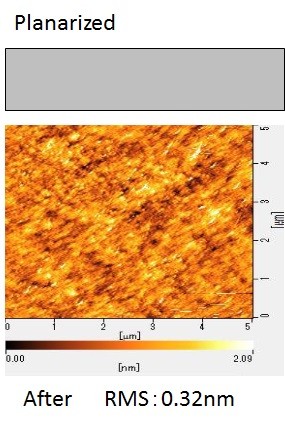
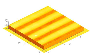
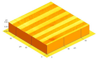
As the number of multilayer wiring layers increases, the irregularities on the IC surface increase and the step becomes larger. The thickened step becomes a film thickness at the time of film forming, the focus at exposure does not match, and it becomes difficult to form a fine pattern. Therefore, CMP is indispensable as surface flattening technology.
Application of CMP
Flattening of interlayer insulating film
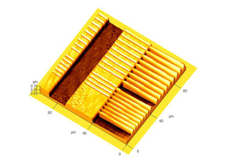
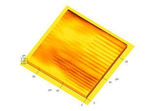
Damascene process
TSV


Improvement of surface roughness before bonding