


Analysis Service
ASSIST-NAVI’s analysis service is a source that supports manufacturing!
Introduction of evaluation equipment


Feature
- Technical staff will propose the optimal analysis method plan according to evaluation purpose.
- We will eliminate waste from the viewpoint of manufacturers and will effectively support problem solving from the field perspective.
- Specialized staff will respond carefully according to specifications needs such as customer’s low budget and short delivery time with flexible correspondence.
Optical interference type film thickness measuring equipment

Measurement of various film thickness in semiconductor process.
Measurement object : SiO2 (silicon oxide), Si3N4 (silicon nitride), resist, Poly Si (polysilicon),
Polyimide / measurement range 10nm to 20um (depending on film type) / measurement accuracy 0.1nm : film thickness 10nm to 3um, 0.03% : thickness 3um to 20um / measurement time : about 1 second.
Surface roughness measurement “Micro shape measurement”

Sample size : 600 x 100mm, Vertical resolution : 0.08nm
Measurement length : 0.08 to 8.0mm and arbitrary length every 0.001mm.
Thin film thickness measurement “fine shape measurement”

Scanning distance 50um to 50mm / stylus radius 2.5um / maximum sample thickness 45mm / Sampling time 1 to 50sec / stylus pressure 1 to 40mgf.
Ultra-deep profile measurement microscope (color laser microscope)

Three-dimensional shape measurement / film thickness measurement
Observation magnification by 50 to 16000 times / Real color three-dimensional surface analysis function / Surface shape measurement resolution 0.01um.
Micro hardness tester

Micro Vickers hardness test
Vickers indenter / test load 0.001 to 2kgf / cavity automatic measurement is possible.
Surface resistivity measurement

High precision measurement by 4 terminal 4 point probe method
[Ω], [Ω/□], [Ωcm], [S/cm] measurable.
Scanning Auger electron spectroscopic analyzer

Analysis of micro surface of semiconductor surface / Metallic multilayer thin film depth direction analysis
Field emission type electron gun / coaxial type cylindrical mirror energy analyzer / multi channel plate detector / analysis mode : point analysis, line analysis, surface analysis, depth direction analysis.
Transmission electron microscope (TEM)
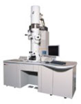
Reflected electron beam diffraction / Transmission electron microscope observation / Restricted visual field diffraction / RHEED
Magnification 50 to 1 million times, acceleration voltage : 200 KV, photographic development type, with energy dispersive X-ray spectrometer (carbon to uranium).
Scanning electron microscope (SEM with low vacuum)

Surface and internal observation equipment.
W filament type, acceleration voltage : 1 to 30.0 KV, resolution : 3nm (acceleration voltage : 30 KV) 15nm (acceleration voltage : 1KV), stage 80*40mm, low vacuum function.
X-ray CT scanning equipment

X-ray tomography
Direct and oblique CT function mounted / Maximum tube voltage 160KV / Focal size 1um (High resolution 0.4um)
X-ray stress measuring equipment

Measurement of residual stress of metal (crystalline) material etc. using X-ray diffraction.
W filament type, acceleration voltage : 1 to 30.0 KV, resolution : 3nm (acceleration voltage : 30KV) 15nm (acceleration voltage : 1KV), stage 80*40mm, low vacuum function.
FIB-SIM (Scanning Ion Microscopy) observation

The accelerated gallium (Ga) ion beam is focused, secondary electrons generated by scanning the surface of the sample are detected and observed as SIM (Scanning Ion Microscopy) image, and precision section machining with nanometer accuracy is possible. It is also suitable for observing crystal grains. Since you can work while confirming the image, you can identify the specific position such as foreign matter adhesion part and internal defects and process it quickly. In addition, high-resolution TEM and FE-SEM observation can be combined with more advanced observation.


