


Our standard TEG wafer (chip) specifications
We have a standard TEG wafer for evaluation such as PKG development, mounting method development, mounting & inspection equipment development, material development etc.
We can also produce TEG wafers (chips) according to customer’s application.
*We also began offering wafer sizes φ300mm (12 inch).
Our standard TEG wafer (chip) specification
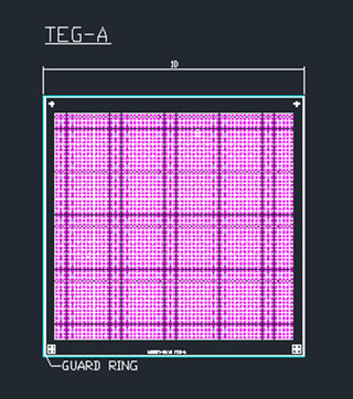
TEG-A

TEG-B


TEG-C


Cross-sectional structure (Scale to be ignored)

Our standard TEG wafer (pad・bump) specification
|
Item |
Bump specification |
Remarks |
|
TEG-□-WB |
Aluminum pad | Optional electroless Ni / Au plating process is also available. |
|
TEG-□-Cu |
Cu post (pillar) plating |
Optional solder bump plating is also supported. |
|
TEG-□-SAC-B |
Solder bump (Lead free) |
|
|
TEG-□-SAC-E |
Ni plating / solder bump plating (Lead free) |
*A, B, C enter into □.
Shipping form
Wafer
- Until passivation formation
- Until polyimide formation
- Solder ball mounted
(including solder plated products)
Delivery form
- Wafer
- Dicing processing, tray packing
- Dicing processing, taping packing
*Board mounting is also available.Please contact us.
Other TEG
Besides WLCSP, we can also offer TEG below.
・ Comb pattern TEG for migration test.


