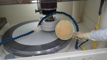
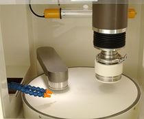
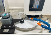
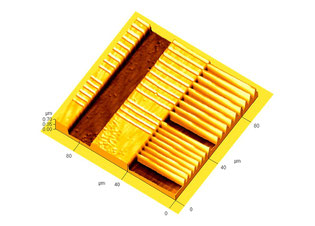
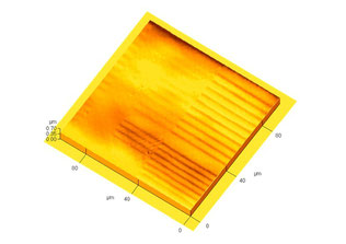
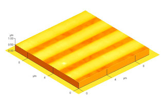
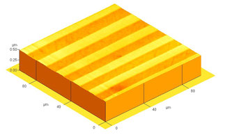
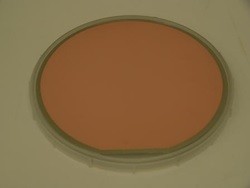
CMP processing
CMP(Chemical Mechanical Polishing)is an essential technology for manufacturing multi-layer wiring boards.
We will introduce the scope of application of CMP with processing examples.
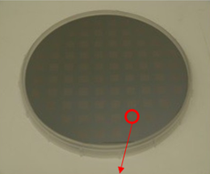
CMP
・Available in sizes from 2 inches to 12 inches.
・Also compatible with square and small boards.
・You can choose the slurry that best suits your application.
・Polishing of glass and ceramic substrates is also possible.
Use it these situations
・Unsatisfactory polishing speed.
・Many scratches, narrow process margin.
・I want the selection ratio
・For those who are dissatisfied with existing CMP slurries.
・Those who want to evaluate pads and slurries.
・Those who want to carry out small-lot processing such as
prototype development.
Features
・We develop products to meet our customers, and processing
conditions.
・From our extensive lineup, we select the slurry and pads that
are best suited to the processing process.
・It is also possible to fine-tune the rotation speed and pressure
during processing.
Purpose of CMP
In multi-layer wiring, the more layers there are, the greater the unevenness and steps
on the IC surface become.
As the step size increases, problems arise during film deposition and resist formation,
making it difficult to from fine patterns.
For this reason, CMP, which flattens the surface irregularities, has become an essential technology for making processing smoother and producing more multi-layered wiring.
The CMP is also used to:
・Flattening the substrate surface when bonding substrates.
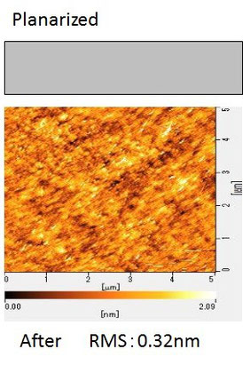
・Mirror finish-Reduces surface roughness of substrate.
・Reduces surface imperfections such as scratches and particles.
Applications of CMP
Planarization of interlayer insulating film

Damascene process
TSV

Improving surface roughness before bonding