


About Nanoimprint
Introduction
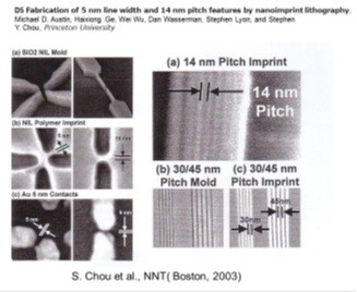
At the node scale below 100nm, many lithography methods including 193nm immersion exposure technology, EB exposure technology, EUV exposure technology, and nanoimprint are being studied. Among theses options, nanoimprint technology attracts attention because it does not require expensive exposure equipment. The study of imprint starts with research of Dr. Chou of Princeton University in 2002. Dr. Chou showed the gate pattern of 5nm width and the patterning result of 14nm pitch in 2003 at NTT (Nanoimprint International Society), and showed that ultrafine processing is possible by nanoimprint technology.
Imprint lithography can be roughly divided into thermal imprint and optical imprint. Thermal imprint is a method of softening the resin at a temperature higher than Tg, and pressing the mold for patterning. On the other hand, optical imprint is a method of pressing a transparent mold against liquid resin and irradiating with UV light to photo-cure. Each method has advantages and disadvantages, and it is necessary to use properly according to the process.
Thermal imprint
Thermal imprint is a method of softening the resin at a temperature higher than Tg, and pressing the mold for patterning. The process flow is shown below.
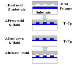
First, apply the thermoplastic resin to the board, bake it and solidify it. Set in the imprint equipment, and heat the board with a hot plate. If the resin temperature exceeds Tg, the resin becomes soft. Therefore, press the mold and perform patterning. When resin temperature is lower than Tg, resin solidifies and the pattern is fixed. Then relax the pressure and release the mold. At that time, depending on the type of resin, heating temperature, pressing pressure, pressing time etc. are process parameters. Since thermal imprint presses the mold against solid resin, the press pressure is relatively strong, usually around 10MPa.
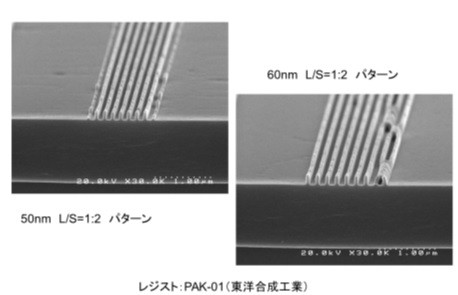
Below is a transfer example of thermal imprint.
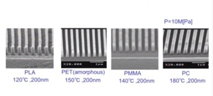
It can imprint at a relatively low temperature of 120℃ for PLA, but high temperature imprint at 180℃ is required for PC.
Optical imprint
Optical imprint is a method of pressing a transparent mold against liquid resin and irradiating with UV light to photo-cure it. The process flow of optical imprint is shown below.
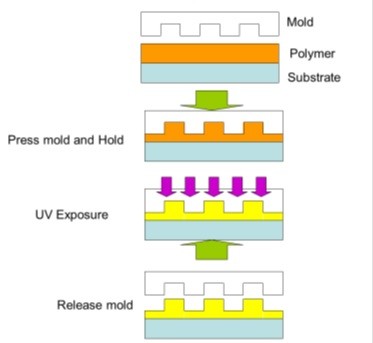
In optical imprint, apply a photo-setting resin to the substrate. At this time, it seems that baking is not often done. Press a transparent mold such as quartz on this board. In the case of optical imprint, since the resin is liquid, imprint is performed in a vacuum environment in order to prevent the contamination of air into the resin. In addition, by using a compressible gas such as PFP (Pentafluoropropane), a process of preventing the contamination of air is also being studied. In optical imprint, since the mold is pressed against a liquid resin, the pressing pressure is not so strong, usually about 0.1 MPa.
Below is a transfer example of optical imprint.
Problem of imprint
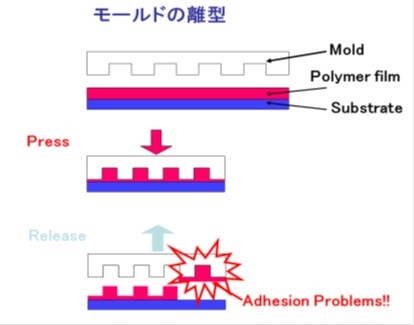
In the case of imprint technology, patterning is performed by directly contacting the mold with the resin. Because of this, if proper mold release treatment is not performed on the mold surface, mold release defects may occur during demolding. This is shown schematically below.
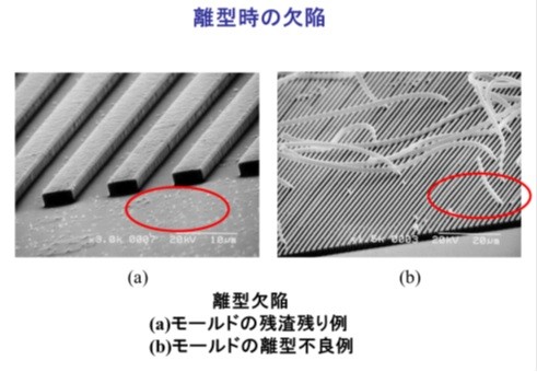
In addition, the following shows an example of occurrence of mold release defects during demolding. (a) shows occurrence of release residue, and (b) shows occurrence of pattern peeling due to release failure.
In order to solve these problems, apply a release agent to the mold surface and apply a mold release treatment. In general, silane coupling treatment with optool material is effective.
Imprint application
As applications of imprint technology, MEMS, bio-elements, optical elements such as polarizing plates, anti-reflective substrates with moth-eye structure, etc. are being studied. Especially, it can be applied to anti-reflective substrate by moth-eye structure. When light travels from the air into the glass-like medium, reflection and refraction will occur on the glass surface. For example, when a glass plate is placed on the screen of a personal computer, the screen reflects and becomes invisible. Therefore, if the glass surface is made into a moth-eye structure, as the light advances from the air to the glass medium, apparent refractive index gradually changes and reflection is suppressed. Therefore, the size of the protrusion of the moth-eye structure requires a fine structure of about 200nm shorter than the wavelength of the light. The moth-eye is “the eye of the moth” and the surface of the “moth’s eyes” has such a myriad of protrusion structures. Therefore, it is said that moths can fly freely at night.
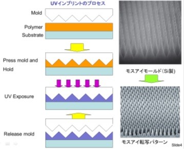
The following shows how to make a moth-eye panel. Apply light curable resin to the surface of the film and push the mold from the top. When UV light is applied, the resin hardens. When peeling the mold, a moth eye structure is made on the surface of the film.
This technology has already been put to practical use, and it is used in LCD television and personal computer.
Summary
Since nanoimprint technology does not require expensive exposure equipment and has high resolution, it is expected to be applied to semiconductor devices such as CMOS in the future.


