


Plating Process
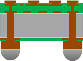
Through-silicon via (TSV)
Compatible with high density and high functionality of the system (towards 2.5D, 3D)
| Wiring layer (standard specification) | |
| Number of layers | Two front and two back layers |
| *Three layers of front and back under development | |
| Insulating material | Polyimide |
| Phenol type resin | |
| Also compatible with low temperature curable resin | |
| Insulation layer thickness | 4 to 10um |
| Wiring material | Cu,Ni,Au |
| Wiring line & space | Min 10/10um |
| Via diameter / Land diameter | 10/40 um |
| Through silicon via (TSV) (standard specification) | |
| Substrate | Silicon substrate 4,6,8 inch |
| Substrate thickness | 300um < |
| *150um under development | |
| Hole diameter | φ50um |
| Hole pitch | > 100um |
*We also support products different from the above specifications.
Please also see “What is through silicon via (TSV) filling?” explained through silicon via (TSV) filling.


