


What is sputtering?
Typical film forming method of PVD (Physical Vapor Deposition).
A method in which high-energy argon ions are bombarded to targets of various materials such as precious metals in a high vacuum, and metal atoms which are struck by argon ions are deposited.
We offer thin film by various sputtering as one method of consignment film forming.
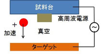
Principle (DC sputtering)
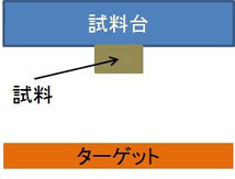
- Set the sample (substrate) to which the film is to be applied and the raw material of the film (target) in the equipment.
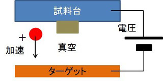
- Vacuum the inside of the equipment, apply a voltage between the substrate and the target.
- Argon gas is put into equipment and ionized by making plasma.
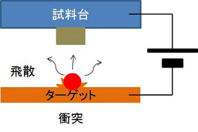
- High-speed accelerated argon ions collide with the target.
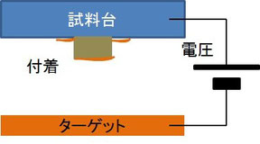
- The particles of the target struck by the collided ions adhere to the substrate and become a film.
About various sputters
DC sputtering

<Advantages>
- The energy of the particles as the raw material of the film is large and the adhesion to the substrate is strong.
- Film can be formed without changing the composition ratio of raw materials of alloy and compound.
- Film forming of high melting point material which is difficult by vacuum deposition.
- Deposition of reactive gas enables film formation of oxide and nitride.
- By applying electric power to the substrate side, it is possible to clean the substrate (reverse sputtering).
- The deposition rate is faster than other sputtering.
<Disadvantages>
- Ions will deposit on the surface of the insulator target and discharge will not occur.
- In order to get electric discharge, the degree of vacuum in the equipment is relatively low, and it is susceptible to the influence of gas.
- The substrate is damaged by the plasma.
- Anomalous discharge is likely to occur.
RF sputtering
<Advantages>
- The energy of the particles as the raw material of the film is large and the adhesion to the substrate is strong.
- Film can be formed without changing the composition ratio of raw materials of alloy and compound.
- Film forming of high melting point material which is difficult by vacuum evaporation.
- Introduction of reactive gas enables film forming of oxide and nitride.
- By applying electric power to the substrate side, it is possible to clean the substrate (reverse sputtering).
- Insulation film can be made.
<Disadvantages>
-
Film forming rate is slower than DC sputtering.
- Since the power supply and the matching box are necessary, the equipment becomes expensive.
Ion beam sputtering
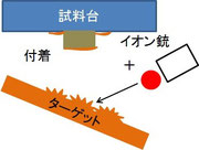
Unlike the above two methods, a film forming method without discharge.
Ions which are released from the ion gun bombard the target, and particles are ejected.
<Advantages>
- It is not necessary to make plasma by discharge, so film forming in a high vacuum environment is possible. Consequently, impurities are less contaminated.
- It is possible to set conditions that are not affected by the conductivity of the target.
- Ultra thin film (10nm or less) can be formed.
<Disadvantages>
- Film deposition rate is slower than DC and RF sputtering.
- Since the mechanism becomes complicated, the equipment becomes expensive.
Application field of sputter deposition
・ CD/DVD ・ Semiconductor ・ Magnetic head
・ Liquid crystal related (transparent conductive film)
・ LED ・ Photocatalyst ・ Battery
・ Various MEMS


